 |
MODIFICATIONS FOR ICOM IC-275A/E/H, IC-475A/E/H, IC-575A/E & IC-1275A/E
OZ1DOQ/PA5DD
Version: 20101231
Recent changes: Note concerning SWR protection added to power control
modification 20101231
RESTORATION OF PASS BAND TUNING
SPLITTING INTO RX- AND TX PATHS
MODIFICATION OF CW PASS BAND (BFO)
Problem:
The original 144 MHz power module (ICOM SC-1013, driver in IC275H) is very likely to fail because of cracks in the ceramic substrate. This is a well-known failure in (early) power modules of this type, and I have had two of these modules fail. The signs are (normally intermittant) loss of output power, typically during heavy use (WSJT or in contest).
Solution:
Simply replace the module with an equivalent type. This would for example be Mitsubishi M57727 (37W), but not M57713 (17W). Altough M57713 will deliver the neccessary output, it will impair the intermodulation charcteristics (IMD) of the transmitter. M57727 is still available from RF PARTS. As the bipolar modules become unavailable, there will be MOSFET replacement. They are however not "drop-in" compatible, and their IMD data also appear inferior to the bi-polar modules.
Problem:
The power control circuit in IC-x75 is an ALC circuit. ALC
circuits suffers from several drawbacks:
- slow reaction time due to time constants
- insufficient regulation due to low feed-back factor
These factors gives the problem that if the average power has
been set to a low value (e.g. for driving a HPA), peak power can
still be in the order of 3-4 dB higher. This leads to either
considerable side band distortion or a low average power output.
note: If you are always using your transceiver barefoot,
without connecting any PA or transverter, this modification will
offer no benefit.
Solution:
The solution to these problems is to use a simple forward gain
regulation without the feed back circuit of the ALC. The original
ALC is still kept for SWR protection only.
The ALC is working on gate 1 of Q13, which is a IF amplifier (9 or 10.75
MHz). The new power regulation uses gate 2 of Q13. Therefore the two circuits
can exist in parallel (see note at the end, though).
The modification should also give you a bigger dynamic range
in the power regulation (lowest power < 5W on the IC-x75H).
Implementation:
- replace R87 (470k) with 100k
- cut "POCO" wire (pin 3, P1/J1, MAIN, orange) at the plug (P1)
- connect the "POCO" wire to gate 2 of Q13 (e.g. via top of R87)
- adjust R250 (SWR protection), R256 (low power level) & R259 (high power level) fully counter-clockwise. SWR protection is now at its maximum. To not have an over-sensitive SWR protection disconnect the antenna and adjust R250 clockwise until the output power increases a bit.
- put the front plate RF PWR in full output position (clockwise) and adjust R82 (Q13 output attenuator) until you have the nominal output power (initially the output power will be higher because you removed the regulation, but the PA will be saturated).
- the balance between FM, CW & SSB output can be adjusted with R137 (CW carrier level) & R105 (FM carrier level).
NOTE: If you often experience a bad SWR condition, you might notice that the ALC SWR protection has an annoying "hang effect". This means that the output power hangs at a certain level until the ALC capacitor has discharged. In some conditions the SWR trigger could even increase the output a bit before it hangs. If you experience problems with this behaviour you should move the SWR protection to gate 2 of Q13 by implementing the modification below. The problem that I have had with this was when driving a tube amplifier on a power generator on the edge of its capacity.
- remove potentiometer R250
- connect a wire between the collector of Q42 (the "single hole side" of the removed R250) and gate 2 of Q13 (e.g. via top of R87, together with the "POCO" wire)
RESTORATION OF PASS BAND TUNING
Problem:
ICOM has chosen to remove the PBT in the later models, and
replace it with a "data level adjustment". This change
removes the possibility to profit from the PBT in case of QRM or
to use the PBT as a cheap CW-filter.
Furthermore the two extra IF-mixings is done with only a
minimum of filtering, making the receiver very susceptible to
spurious IF breakthrough. This is often heard as high-pitch tones
or as a high IF noise level.
Solution:
The solution is to re-wire the "data level" potentiometer so that it adjusts
the PBT VXO-oscillator, and to re-install FI3. FI3 is a 455kHz ceramic SSB
filter and can be bought under the type number: MURATA CFJ 455 K5 or CFJ 455 K6.
Implementation:
- remove the capacitor (C61) fitted in place of FI3
- solder in FI3
- readjust R72 for proper IF gain
- cut wire PBTV (pin 4, P1/J1, MAIN, yellow) about 5cm from the plug (P1)
- cut wire AMO2 (pin 4, P2/J18, MAIN, red) close to the plug (P2)
- cut wire AMO3 (pin 3, P2/J18, MAIN, metal baird) close to the plug (P2)
- connect PBTV wire (the 5cm long stub connected to the plug) with AMO2 wire (the end not connected to the plug)
- connect AMO3 (the end not connected to the plug) to +8V e.g. by tapping (pin 1, J4, MAIN, brown).
- connect the wire stubs on the plug (AMO2 & AMO3) together is you wish to use external modulation input for PACKET etc.
- adjust the coil next to X2 (PBT VXO) for correct middle PBT
setting
SPLITTING INTO RX- AND TX PATHS
Problem:
This is a general transceiver problem. If you want to use the
transceiver as part of a bigger setup (i.e. with external PA
& preamp or with a transverter), it is convenient to have
separate access to the RX and the TX of the transceiver.
Otherwise you need two coaxial switches every time you add a new
accessory. With split RX/TX paths you only need one switch - at
the antenna. Furthermore split RX/TX paths eliminates the need
for a change-over sequencer.
On the other hand it is also nice to have the transceiver
working normally when you are using it barefoot.
Solution:
The solution is to jump wire the RX path (between RX and the
RX/TX switching) trough the rear side of the transceiver with 2
BNC connectors. In normal state these connectors are connected
via a short cable. In case you need to "split up" the
transceiver, you remove the short coax cable, and you obtain
direct access to the RX. The TX is still available using the
common connector.
note: If you are always using your transceiver barefoot,
without connecting any PA, preamp or transverter, this
modification will offer no benefit.
|
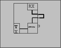
Remove the back cover. If you place the holes for the BNC
connectors next to and aligned with the two existing
DIN-connectors, then ICOM have left enough space on the inside
for the connections. You can also add other desired outputs like
a phono plug for AF OUT.
The RX cable runs between J4 on the RF YGR PCB and the PA
unit.
note1: In my IC-275H the PIN-diode for the FM RF gain is shared
with the RX/TX switch and placed in the PA unit. This means that
the control voltage passes through the RX cable. Therefore the
breaking of the RX cable will cancel the FM RF gain function (the
SSB/CW RF gain is working on the AGC and is not affected). The
solution is to install a new PIN-diode (D5) on the RF-YGR PCB.
The PCB has already room for it. To avoid short-circuiting the
control voltage the jumper placed in stead of C86 on the RF-YGR
PCB, should be replaced by a 1nF capacitor.
note2: Using this spilt RX/TX configuration I have observed problems with oscillation when using an external preamp, that is left on during transmit. This can been seen as a small and constant amount of output power, when the rig is transmitting. Apparently there is some internal coupling between the RF RX and TX paths, or the IF switching does not have sufficient isolation. Given the total gain of the TX path, the external preamp and limited isolation of the antenna relay an oscillation condition can occur.
The solution is to activate the input attenuator (designed for RF GAIN in FM
mode) during transmit. This done by connecting a 1N4148 diode in series with a
1k ohms resistor from "T13" (red wire going on to the board) on RF YGR board
to "FRFG" (pin3, J1, RF YGR board). The installation is best done under the RF
YGR board. The anode of the diode should face “T13”. The better solution is to
cut the supply to the preamp during transmission.
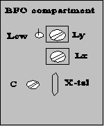
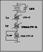
MODIFICATION OF CW PASS BAND (BFO)
Problem:
In these transceivers ICOM has chosen to shift the CW passband
up 200 Hz compared to the SSB passband. This makes it more
difficult to copy SSB signals in CW mode.
Solution:
The extra BFO coil that is added in CW-R is short-circuited,
and the BFO is re-adjusted for proper CW RX/TX-tracking and for
preferred USB/CW passband.
Implementation:
- short-circuit Lcw in the BFO compartment.
For readjusting the BFO you need another transceiver (TRX2)
with correct tracking.
1. Receive on TRX2 and transmit in CW. Adjust the VFO (with
the RIT off !) of TRX2 until you have the desired side tone in CW
mode. (e.g. 800 Hz - can be found by beating the tone with the
side tone oscillator).
2. Transmit on TRX2 and adjust Ly (CW-R) until you have a 800 Hz tone in CW mode. (you are setting the difference between CW-R & CW-T).
3. Adjust Lx (CW-T) for preferred USB/CW receive passband.
You might have to repeat the tuning once again, as there is some interaction between the adjustments. If you would like to adjust the LSB passband, this should be done by adjusting the capacitor C, before adjusting the coils.
 |
 |
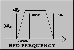 |
Note: The BFO coils are switched in successively to give the
required offset from the LSB frequency. Therefore adjusting CW-T
also changes USB/CW-R.
Re-adjusting all of the BFO frequencies is a good idea in any
case to compensate for crystal aging. If the passbands sound
different in LSB and USB it is a sure sign of mis-alignment due
to crystal drift - they should be more or less the same.
Problem:
Squelching is nice to have in FM mode, but it doesn't really
work for SSB, where you will be looking for weak signals.
Therefore you have to adjust the squelch level every time you
change mode. Furthermore I enjoy using FM as a monitoring mode on
the SSB calling frequency, so changing the mode happens quite
often.
Solution:
The solution is quite simple. Just cut the connection to the
SSB input of the squelch circuit in some way.
Implementation:
The easiest way to break the connection is to connect the base
of Q7 to ground. The base is the lead facing into the centre of
the PCB.
Problem:
For some modes of weak signal communication, it can be
desireable to have a very fast AGC (e.g. meteor bursts with a
sharp rise and a long weak "tail"). The standard fast
AGC has a time constant of about 2 secs (!), which also means
that a noise pulse can mute you for quite some time.
Note: Never use the noise blanker when receiving high speed CW
(Meteor Scatter). The noise blanker mistakes the high speed
keying for noise pulses, and will seriously corrupt the signal.
Solution:
The solution is to move the "AGC fast" capacitor
(C19) to replace the "AGC slow" capacitor (C20) on the Main
board. You
will loose the "AGC slow" option, but I find "AGC
fast" adequate for most signals.
Another solution is to switch out the "AGC fast"
capacitor (C19) seperately, but then you will get the problem of
finding an appropiate front plate switch. I already tried to use
the DATA button, but it cannot be activated in CW.
note: a strong signal will be seriously distorted in AGC fast
mode.
Implementation:
- remove C20
- move C19 to the replace C20
AGC OFF (for use with WSJT/FSK441) can be achieved by adding a back panel switch, that disconnects the emitter of Q9 on the Main board. The base (the pin on Q9 facing outwards) is de-soldered and lifted upwards. A wire is soldered in the empty hole, and another wire is soldered to the emitter. When the two wires are disconnected from each other the AGC is off.
The dynamic range of the AF signal output to WSJT depends on the RF & IF gain before the AF amplifier (R72 adjusts the IF gain) . If there is too much gain, the AF amplifier will staturate, and there will be no dynamic range in the output signal for WSJT to trigger on. Be sure to regulate the gain, and a dynamic range of >10dB will be achievable. This is a big improvement over the AGC case, where the output will be constant as soon as the AGC threshold level is reached.
Problem:
The RF GAIN function is different in FM and in SSB/CW modes.
In FM mode the RF GAIN controls a PIN-diode at the input of the
preamp. In SSB/CW the RF GAIN simply activates the IF AGC.
The use of the preamp input attenuator (the PIN-diode) can be
useful also for SSB/CW e.g. if you have connected a mast head
preamp with excessive gain. In this case the attenuator will help
you to adjust the signal levels at the mixer, and thus reduce
intermodulation and blocking.
Solution:
The solution is to remove the SSB/CW RF GAIN for SSB/CW (this
function is of little use anyway), and enable the FM RF GAIN even
in SSB/CW.
Implementation:
- Cut the lead (FM8V) conneted to (pin5, J6, potmeter PCB, green) about 4 cm from the plug
- Connect the short plug end with R14 (on the potmeter PCB) by
soldering it to the end that is connected to the plug (+8V)
This will enable the FM RF GAIN in SSB/CW.
- cut R30 open
This disables the SSB/CW RF GAIN, and you now have a variable
input attenuation with a dynamic range of 10dB (IC275 with
MI308/1nF) to 16 dB (IC475).
note: The IC-275 might have a shared PIN diode for FM RF GAIN
and TX/RX switching. If you choose to split up the RX/TX paths,
you must install a new PIN diode (MI301 or equivalent) on the RF
YGR PCB to implement this modification. See the note under the
section dealing with spliting the RX/TX paths.
Do not mount a crystal heater to the 30.72 MHz reference oscillator
The ICOM CR-64 high stability oscillator is quite expensive, so I tried to
improve the stability of the standard crystal oscillator by adding a crystal
heater from the
DB6NT.
This was not a succes. The crystal is obviously designed for room temperature,
and the stability at that temperature is actually very good. By raising the
temperatur to 40° C using the crystal heater the stability gets much worse.
The tunning speed is set to a defaults of 100Hz, 1kHz, 5kHz or
1MHz depending on front plate setting and mode. These settings
can be manipulated by D41 - 46 at the front plate. At least a
setting of 10kHz is also available.
The IC-275 have capability to cover 138 - 174 MHz and the
IC-475 has capability to cover 430 - 450 MHz. Because of hardware
restrictions they might not be fully up to specifications in all
of the band, but an extended range can be interesting for e.g.
use with a transverter. It seems that the IC-275 has a parallel
wide band preamp, that can be switch via the WBT pin on RF-YGR
PCB.
In the European versions the transceivers are wired for 1750
Hz repeater call, and they have no CTCSS capability. The
transceivers have a built-in CTCSS encoder, so these functions
can be restored.
Both of these version dependent functions can be set by the
diode matrix: D20 - D24 in the logic unit. I do not know the
exact mapping, but a lot can be derived from studying the
different frequency ranges and the diode matrix coding table
found on the schematic diagram.